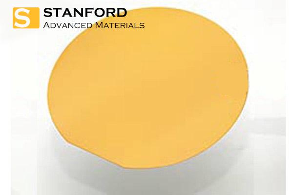
Au/Cr Coated SiO2/Si Substrate Description
Our gold-plated silicon wafers serve as exceptional substrates, extensively utilized in the nanotechnology sector, scanning electron microscopy (SEM), atomic force microscopy (AFM), and various scanning probe microscopy applications. Additionally, they are ideal for cell culture, protein and DNA microarrays, and reflectometry. Each silicon wafer is meticulously coated with a 5 nm layer of chromium, followed by a 50 nm gold film, ensuring superior performance and reliability.
Au/Cr Coated SiO2/Si Substrate Applications
Our Au/Cr coated SiO₂/Si substrates are widely employed in the nanotechnology field, seamlessly integrating with SEM, AFM, and other scanning probe microscopy techniques. They are also pivotal in cell culture experiments, protein and DNA microarray development, and reflectometric analyses, providing a reliable foundation for advanced scientific research and technological innovations.
Au/Cr Coated SiO2/Si Substrate Packaging
Each Au/Cr coated SiO₂/Si substrate is meticulously handled during storage and transportation. Our stringent packaging protocols ensure that the substrates maintain their pristine condition, safeguarding their quality and performance upon delivery.
 Get a Quote
