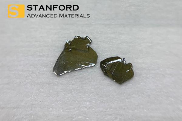
Copper Silicon Phosphide Crystal Description
Copper Silicon Phosphide Crystal exhibits a layered van der Waals (vdW) structure with easy exfoliation characteristics. Despite their layered nature, their fundamental properties remain largely unknown. They are predicted to behave as 2D metals and semimetals when thermally heated or exposed to laser treatment, which can also cause them to convert to a SiP layered phase. More fundamental studies are absolutely needed to establish their electronic, magnetic, and optical properties.
They may possess good thermal stability, beneficial for high-temperature applications. The combination of copper, silicon, and phosphorus can also result in a material with good mechanical strength.
Copper Silicon Phosphide Crystal Specifications
|
Material
|
CuSi2P3
|
|
Crystal system
|
Monoclinic phase
|
|
Unit Cell Parameters
|
a= 0.368 nm b=0.739 nm, c=1.635 nm,
α=48.1°; β=55.965°, γ=60.54°
|
|
Size
|
~3-5mm
|
|
Characterization Methods
|
SIMS, XRD, EDS, Raman
|
|
Purity
|
99.9995%
|
Copper Silicon Phosphide Crystal Application
- Semiconductors: Due to their semiconductor properties, CuSiP crystals could be used in the manufacture of electronic components such as transistors, diodes, and integrated circuits.
- Photovoltaics: They might be used in the development of solar cells and other photovoltaic devices due to their ability to convert light into electricity.
- Alloys and Composites: These crystals could be used to create specialized alloys or composites with unique properties for industrial applications.
- Optoelectronics: Potential use in optoelectronic devices where electrical and optical properties need to be precisely controlled.
Copper Silicon Phosphide Crystal Packaging
Our Copper Silicon Phosphide Crystal is carefully handled during storage and transportation to preserve the quality of our product in its original condition.
Copper Silicon Phosphide Crystal FAQs
Q1: What is Copper Silicon Phosphide (CuSiP)?
Copper Silicon Phosphide (CuSiP) is a compound crystal that combines copper (Cu), silicon (Si), and phosphorus (P). It is known for its semiconductor properties and potential applications in electronics and photovoltaics.
Q2. What is the structure of CuSi₂P₃ crystals?
CuSi₂P₃ crystals exhibit a layered van der Waals (vdW) structure, which allows for easy exfoliation.
Q3. What happens to CuSi₂P₃ crystals when heated?
When CuSi₂P₃ crystals are heated thermally or exposed to laser treatment, they are predicted to behave as 2D metals and semimetals. They can also convert to a SiP layered phase under these conditions.
 Get a Quote
