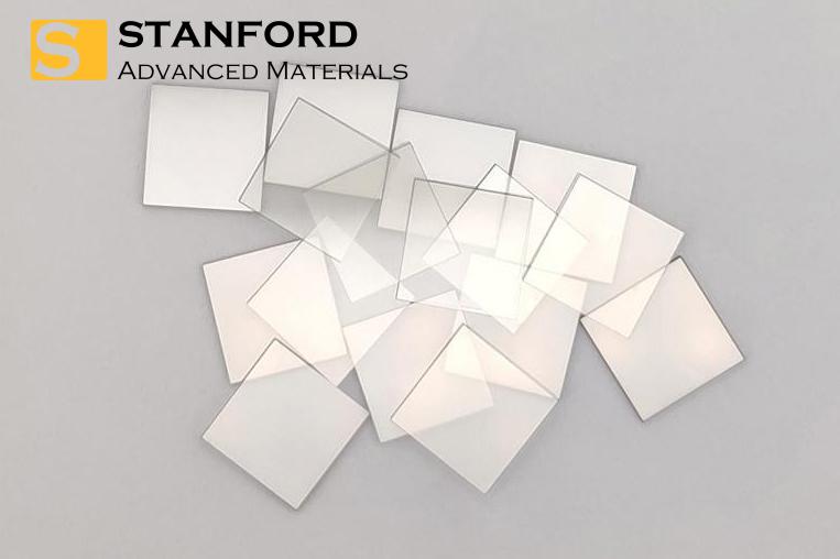
Description
CVD Diamond Wafer exhibits outstanding physical and chemical properties, providing optical transparency across various frequencies from ultraviolet (UV) to terahertz (THz). As a form of carbon, diamond offers the highest hardness and thermal conductivity, along with excellent wear resistance, chemical stability, and radiation resistance. These wafers are suitable for applications involving X-rays, UV, infrared, and microwave frequencies.
CVD diamond wafers are an optimal choice in applications requiring efficient heat dissipation, low dielectric loss, high Raman gain, minimal beam distortion, and resistance to erosion. Their superior thermal conductivity makes them ideal for managing heat in devices with high heat flux, ensuring effective temperature control and preventing critical component overheating.
Applications
CVD Diamond Wafers are used in various industries due to their superior properties:
-
Electronics: Serve as heat sinks and insulating substrates in high-power devices, aiding in effective heat dissipation and electrical insulation.
-
Optics: Used to make optical windows, lenses, and mirrors for lasers and sensors, benefiting from their high optical clarity and durability.
-
Medical Devices: Enhance precision and longevity in surgical tools and dental drills thanks to their hardness and wear resistance.
Packaging
Our CVD Diamond Wafer is carefully handled during storage and transportation to preserve the quality of our product in its original condition.
 Get a Quote
