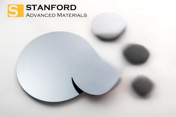
Epitaxial Wafer SiC-GaN EPI refers to a semiconductor thin film grown on a substrate. Stanford Optics has rich experience in manufacturing and supplying high-quality optical products.
|
Wafer Diameter |
4" |
5" |
6" |
8" |
|
|
EPI Layer |
Dopant |
Boron, Phos, Arsenic |
|||
|
Orientation |
<100>, <111> |
||||
|
Conductivity type |
P/P++, N/N++, N/N+, N/N+/N++, N/P/P, P/N/N+ |
||||
|
Resistivity |
0.001-50 Ohm-cm |
||||
|
Res. Uniformity |
Standard <6%, Maximum Capabilities <2% |
||||
|
Thickness (um) |
0.1-100 |
||||
|
Thickness Uniformity |
Standard <3%, Maximum Capabilities <1% |
||||
|
Substrate |
Orientation |
<100>, <111> |
|||
|
Conductivity type/Dopant |
P Type/Boron , N Type/Phos, N Type/As, N Type/Sb |
||||
|
Thickness (um) |
300-725 |
||||
|
Resistivity |
0.001-100 Ohm-cm |
||||
|
Surface Condition |
P/P, P/E |
||||
|
Particle |
<50@.0.5um |
||||
E-mail address with your company's domain name is preferred. Otherwise, we may not be able to process your inquiry.
Please fill in the required fields.