Product Overview
Germanium Sulphide (GeS) is a layered semiconductor known for its indirect band gap near 1.6 eV. Its crystal structure consists of stacked layers held by van der Waals forces, allowing exfoliation into ultrathin 2D sheets. This unique feature places GeS among group-14 transition metal monochalcogenides with distinctive electronic and optical properties.
Stanford Optics supplies high-purity GeS crystals suited for research and development in optoelectronics and nanoelectronics.
Key Features
-
Indirect band gap around 1.6 – 1.65 eV
-
Layered orthorhombic crystal structure
-
High chemical purity (>99.995%)
-
Suitable for exfoliation into thin layers
-
Stable semiconductor properties for device fabrication
Applications
-
Advanced optoelectronic devices
-
Nanoelectronic components
-
2D material research and development
-
Photodetectors and sensors
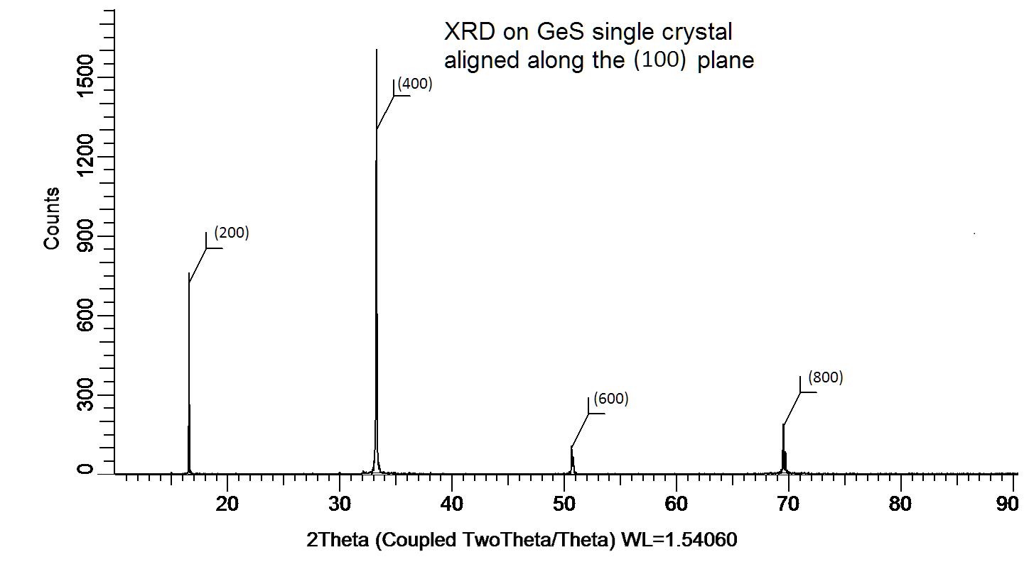
Crystal XRD
Packaging
To maintain crystal quality, our GeS crystals are carefully packaged and handled during storage and shipment. This ensures the material arrives in pristine condition, ready for your applications.
 Get a Quote
 Crystal.jpg "OP4387 Germanium Sulphide (GeS) Crystal")