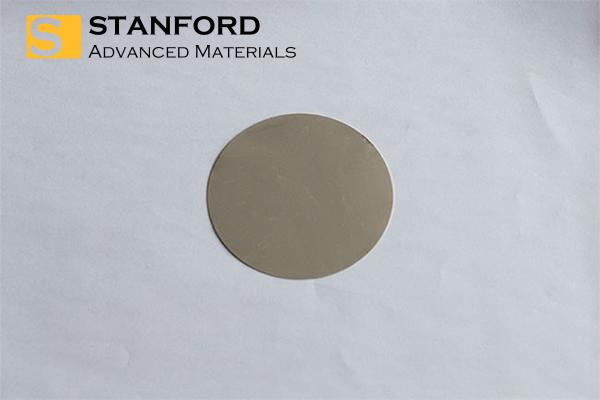
Ni-coated SiO2/Si substrates are ideal for applications in the nanotechnology field, including scanning electron microscopy (SEM), atomic force microscopy (AFM), and other scanning probe microscope systems. Stanford Optics has extensive experience in manufacturing and supplying high-quality optical products.
 Get a Quote
-
- Offshore Wind Farm Connectivity Solutions
- Railway Trackside Communication Networks
- 5G Network Deployment
- Outdoor Surveillance Systems
- Marine Communication Systems
- Long-Distance Communication
- FTTH Network Deployment
- LANs
- Smart Transportation
- Emergency Response Networks
- Data Transmission
- Environmental Monitoring
- Fiber Sensing
- Underwater Monitoring
