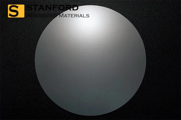
Our Pt-coated SiO2/Si substrate is carefully handled throughout storage and transportation to ensure the product retains its original quality.
Pt Coated SiO2/Si Substrate can be used in the nano field, scanning electron microscopy (SEM), atomic force microscopy (AFM), and other scanning probe microscope ranging. Stanford Optics has rich experience in manufacturing and supplying high-quality Optical Products.
Pt-plated silicon wafers find extensive use as substrates in the nano field, scanning electron microscopy (SEM), atomic force microscopy (AFM), and other scanning probe microscopy techniques. They are also applied in cell culture, protein DNA microarrays, and reflectometers. Typically, the silicon wafer of this product is coated with a layer of platinum (Pt) approximately 150nm in thickness.
These wafers are widely used in various applications, including SEM, AFM, and other types of scanning probe microscopy, as well as in cell culture, protein DNA microarrays, and reflectometers.
Our Pt-coated SiO2/Si substrate is carefully handled throughout storage and transportation to ensure the product retains its original quality.
Composition |
Pt, Ti, Si, SiO2 |
Film |
SiO2 500nm (N100), Pt 150mm, Ti 20nm |
Substrate Size |
4" diameter |
E-mail address with your company's domain name is preferred. Otherwise, we may not be able to process your inquiry.
Please fill in the required fields.