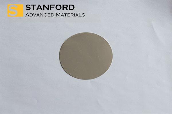
Stanford Optics provides high-quality Ti-coated SiO₂/Si substrates designed for use in nanotechnology, surface analysis, and advanced material science. These wafers feature a thermally grown or deposited SiO₂ layer on single-crystal silicon, over which a controlled layer of titanium (Ti) is deposited via physical vapor deposition (PVD) or e-beam evaporation.
The Ti coating offers excellent adhesion, conductivity, and biocompatibility, making these wafers ideal for surface modification, functionalization, and high-resolution imaging.
Ti-coated SiO₂/Si substrates are widely used in:
Nanofabrication & Patterning
Ideal for e-beam lithography, nanoimprinting, and metal lift-off processes.
Surface Characterization
Suitable for SEM, AFM, and other scanning probe techniques requiring conductive or functional surfaces.
Biofunctional Surfaces
Used in cell culture, protein-DNA microarrays, and biosensor interface studies.
Optical and Reflectometric Analysis
Stable reflective base layer for spectroscopic and optical metrology tools.
To ensure the highest quality, our Ti-coated Ta/SiO2 silicon wafers are carefully handled during storage and transportation, preserving their integrity.
Packing: The wafers are securely packaged in a 1000-class clean room environment within plastic bags to maintain cleanliness and safety during shipping.
Composition |
Ti, SiO2, Si |
Size |
2, 4, 6, 8” |
Composition |
Ti, SiO2, Si |
Ti Film Thickness |
15-100nm, or customized |
E-mail address with your company's domain name is preferred. Otherwise, we may not be able to process your inquiry.
Please fill in the required fields.