Tin Disulfide Crystal Description
Tin Disulfide Crystal is a semiconductor with an indirect band gap of ~2.2 eV. The layers are stacked together via van der Waals interactions and can be exfoliated into thin 2D layers. SnS2 belongs to the group-14 post-transition metal dichalcogenides.
Tin Disulfide Crystal Specifications
|
Material
|
SnS2
|
|
Crystal size
|
~8 mm
|
|
Electrical properties
|
Semiconductor (~2.2eV)
|
|
Crystal structure
|
Hexagonal
|
|
Unit cell parameters
|
a = b = 0.364, c = 0.589 nm, α = β = 90°, γ = 120°
|
Tin Disulfide Crystal Application
Tin Disulfide Crystal is a semiconductor with an indirect band gap of ~2.2 eV.
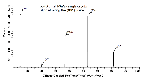
Tin Disulfide Crystal XRD
Tin Disulfide Crystal Packaging
Our Tin Disulfide Crystal is carefully handled during storage and transportation to preserve the quality of our product in its original condition.
Tin Disulfide Crystal FAQs
Q1: What is tin disulfide (SnS2)?
Tin disulfide is a layered compound with the chemical formula SnS2. It is a n-type semiconductor and belongs to the group IV-VI semiconductors, characterized by its yellow hexagonal crystals.
Q2: What are the properties of tin disulfide crystals?
Tin disulfide crystals exhibit properties such as a wide band gap (approximately 2.2 eV), good optical absorption, and high photoconductivity. They are also chemically stable, resistant to oxidation, and non-toxic, making them environmentally friendly for various applications.
Q3: How are tin disulfide crystals synthesized?
SnS2 crystals can be synthesized using several methods, including chemical vapor deposition (CVD), hydrothermal synthesis, and mechanical exfoliation from bulk SnS2. The choice of method impacts the crystal quality, size, and morphology.
 Get a Quote
